isel_icv4030:milling_pcb_s
This is an old revision of the document!
Milling PCB workflow
(experimental)
Using Eagle, Tracespace.io, InkScape and Fusion 360

Nonsense demo circuit and PCB layout
- Make circuit and PCB layout in Autodesk Eagle (version 9.4.0)
File > Generate CAM data- Click OK. This will generate a zip archive with Gerber files (2D vector files used for PCB manufacturing).
- Unzip the .zip file and open the GerberFiles folder.
- Open https://tracespace.io/ to convert the desired Gerber files to SVG vector files.
- Open the desired .SVG files in Inkscape.
- use
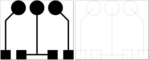
view > display mode > normal / outlineto analyse the vector image.

Seeing the image in the outline display mode (right), it becomes apparent that the traces have a width of zero mm.
edit > select all(ctrl + a)object > ungroup(shift + ctrl + g)- the circles and squares are clones from hidden shapes. select one clone-object.
edit > select same > Object type(shift + alt + a)file > clone > unlink clone(shift + alt + d). The clone objects have now been changed to circle and rectangle objectsedit > select allpath > objects to pathpath > stroke to pathpath > break apartpath > unionfile > save asChoose SVG.
- insert the SVG file in fusion 360
- set scale to
0,003779527597(The dimensions set in Eagle are correct in InkScape, but with scale set to 1, 1,27mm in eagle becomes 336,02083mm in Fusion 360) - select contours, extrude and configure setup and trace operation for milling
isel_icv4030/milling_pcb_s.1562337660.txt.gz · Last modified: by formlab

